Data Sheets
Driven by the Internet of Things, advanced microelectronics are transforming human interaction with the world. From cars and homes to medical and personal fitness equipment, the growing demand for integrated devices requiring advanced technology is rapidly multiplying, powering a new era known as the Fourth Industrial Revolution. As this trend grows, new cutting-edge manufacturing processes are necessary to keep up with the pace of the microelectronics-driven economy. The technology in development at BRIDG is on track to be an enabling domestic force in virtually every industry value chain that delivers a product or service to anyone, anywhere.
-
Accelerate extreme functional density for next-generation products and systems
-
Develop and provide production and commercialization capabilities
-
Provide qualified production technologies for advanced heterogeneous system integration
-
Provide prototyping, custom process development, and low-volume production foundry services
- Flexible IP management and protection
-
Provide academic institutions with capabilities to enable core research with a path to commercialization
-
Provide Digital Twin for Semiconductor methodologies
BRIDG Technologies
-
2.5/3D Device Integration, Interposers, Assembly, and Packaging
-
Ultra-dense High Speed Digital and Radio Frequency (RF) Electronic System Enablement
-
Hardware and system secure devices and processes such as a CMOS-integratable PUF for cryptography
-
Advanced Materials and Device Development Lines – III-V and other novel materials integrated into silicon-based devices
– Sensors, Imagers, RF, Power, and other heterogeneous integrated systems
– Materials Focus – GaAs, InGaAs, InP, GaSb -
Design Center Engineering (enabled via partnership with imec)

By uniting bold ideas with holistic capabilities and production-qualified process technologies, BRIDG enables tomorrow’s advanced innovations to reach the market at a greater velocity than ever before across a multitude of fields.
BRIDG has a world class set of 200mm wafer-processing tools to enable researchers and electronics product companies to develop and produce high performance systems, sensors, and security devices with robust 2.5/3D advanced-system integration, assembly and packaging capabilities. BRIDG also offers a relatively new physically unclonable function (PUF) technology that is very integratable with CMOS devices, enabling next-generation cybersecurity cryptography and uniquification solutions.
Our manufacturing development center is focused on two initial functional platforms:
Advanced Materials and Devices Development Line
- Designed to support a broad range of industries (Biomedical, Agriculture, Environmental, etc.
- Universal Smart Sensors and III-V materials – Multipurpose product applications (ionic, molecular, chemFETs sensor with wireless communication)
Advanced Packaging, Testing, and Device Integration Development Line
- Back-end processing and packaging line for prototype development and commercialization (Biomedical, Oil and Gas, Aerospace/Defense, Environmental, Agriculture Sensors)
- Advanced Optics and photonics devices – wide range of advanced applications (SIP)
BRIDG capabilities will be focused around these initial process technologies:
Advanced System Integration—Includes heterogeneous 2.5D and 3D multi-chip integration with production capabilities for high speed digital and RF silicon interposers, die/wafer assembly and packaging.
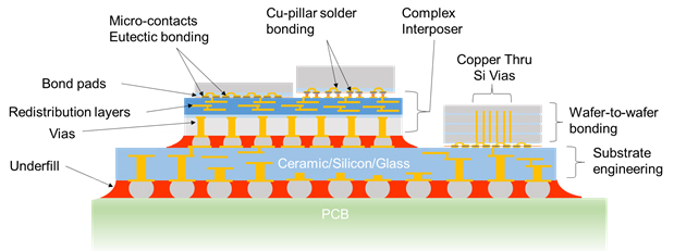
BRIDG’s current photolithography capabilities allow building chip features as small as 0.5 micron, which enables ultra-dense metal interconnect between chips using interposers, redistribution layers of metal wiring, and other techniques. BRIDG plans to acquire additional photolithography tools with capabilities down to 0.05 micron, or 50 nanometers (50nm). As the advanced system integration platform evolves, BRIDG will provide capabilities to support the heterogeneous device integration schemes illustrated below. These capabilities will address complex and diverse needs required for system integration.
PUF Process Technologies—Enables a very unique, resistance-based, Physically Unclonable Function (PUF) capability in large addressable arrays, which is positioned to be a key hardware security root-of-trust for next-generation systems by enabling more robust cryptography and chip-level “fingerprinting.”
PUF Process Technologies
Among the first chip process technologies that BRIDG is concentrating on is an interesting resistive memory-based process. This process enables the creation of a high entropy an array of unique PUF (physically unclonable functions) cells from resistive elements instead of transistor-based memory bits. These PUF devices are also very low power and are currently being evaluated for radiation hardness (radhard).
III-V Technologies—Enables the production of wafers with special crystalline materials “grown” on top of a wafer from the III and V groupings on the periodic table of elements, such as gallium arsenide (GaAs), indium phosphide (InP) and indium gallium arsenide (InGaAs), and are useful for creating functions like lasers, photocouplers, radio-frequency devices and many types of sensors and other devices.
III-V Technologies
BRIDG enables open innovation platforms using advanced materials and device development lines, which can accelerate the commercialization of new sensors and other technologies. BRIDG’s technology initiatives in III-V deposition tools and other materials pave the way for sensors, photonics, optics and advanced integrated devices to support diverse industries, including biomedical, agriculture, environmental, and RF communications. BRIDG currently offers epitaxial growth of III-V materials such as GaAs and InP on 150mm and smaller wafers. Over time, BRIDG will also offer lithographic device processing capabilities on these smaller wafers. BRIDG also has an initiative in process to provide GaN epitaxial growth and device processing on 200mm wafers, which would make BRIDG one of very few places in the world with open GaN foundry capabilities of growth and processing under one roof.
Leading-Edge Technology Development—Provides access to BRIDG’s arsenal of semiconductor processing tools for photolithography, deposition, etching, doping, cleaning, metrology and testing. These numerous and diverse tools for chip production are the production backbone of the semiconductor industry and are each very complex machines by themselves.
Leading-Edge Technology Development
BRIDG plans to acquire additional tools over the next several years ensuring it to be more advantageous and attractive for manufacturers from health, aerospace, defense and other industries. While a solid set of the core tools at BRIDG are now installed and qualified for use, the list of additional tools being planned and considered for future technology platform growth is long. The expansion capabilities for BRIDG have been planned from the beginning to be significant and flexible.